
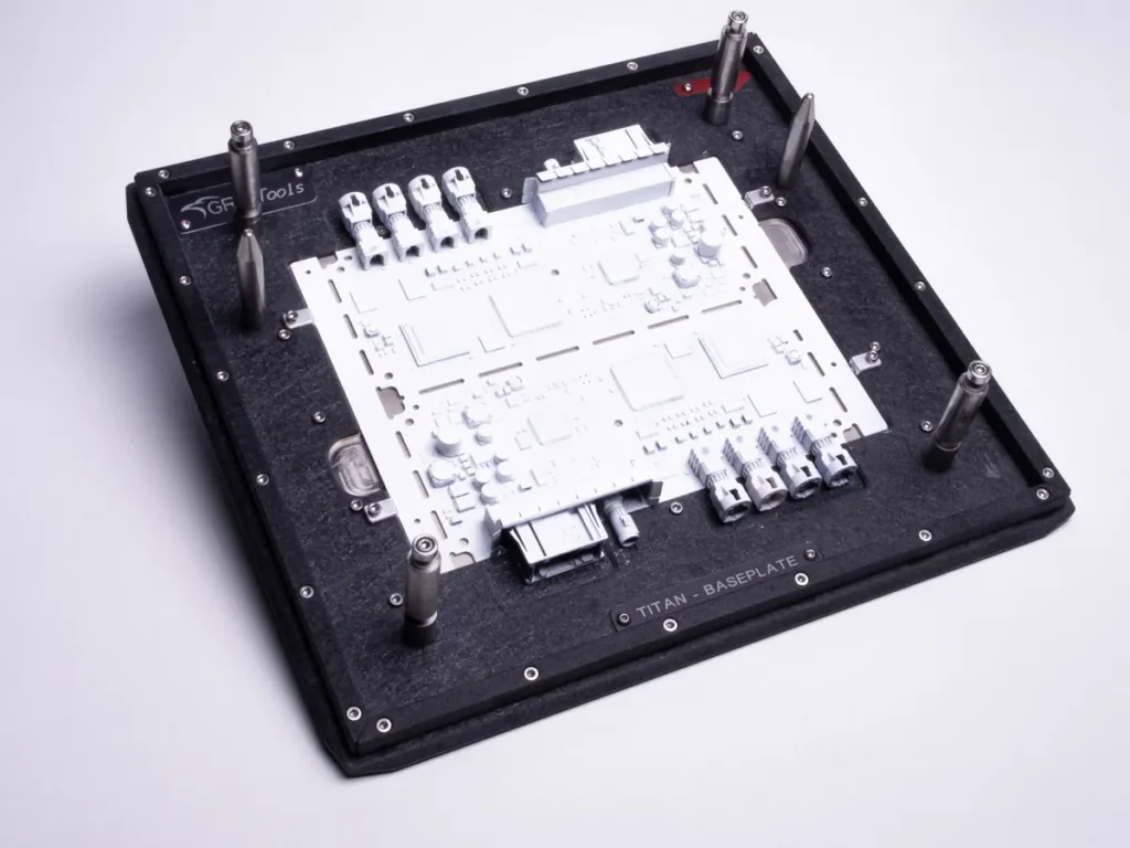
A wave solder pallet (or carrier) holds your PCB over the solder wave, masks the areas that must stay solder-free, and presents the right components to the wave at the correct height and angle. A pallet that fits your board and your machine is the difference between a clean, repeatable process and constant touch-up.
Start from the board and the machine
Every pallet is engineered to a specific board layout and a specific wave or selective machine. We work from your Gerber, STEP, DXF, ODB++ or HPGL data together with the target machine, so the pallet drops straight into your line with the correct rails, fingers and clearances.
Mask what matters, expose what needs the wave
Keep-out zones, connectors, press-fit areas and tall components all shape the pallet geometry. We design the openings so the wave reaches exactly the joints that need it, while sensitive areas stay protected — reducing bridging, shadowing and rework.
Built for repeatability
Durable tooling materials, precise location and clear handling keep the process consistent from prototype to series. If you have a board and a process in mind, send us the data and we will confirm what is needed.