
Custom wave solder pallets & THT carriers
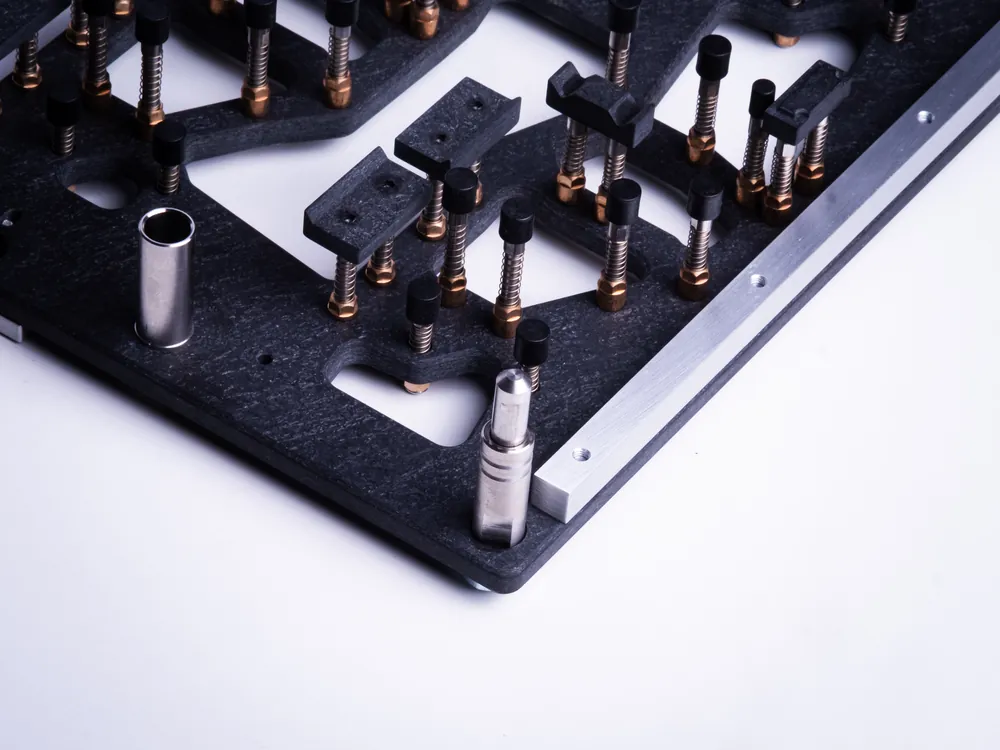
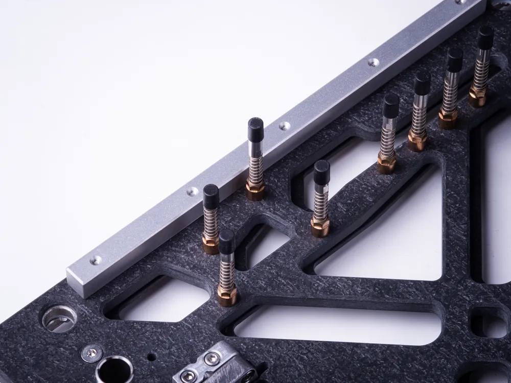
A wave solder pallet (or solder carrier) masks the areas of a PCB that must not meet the solder wave while exposing the joints that should. Griftools designs each pallet around your board, your through-hole layout and your wave or selective machine — so the result is repeatable on the line, not just correct on paper.
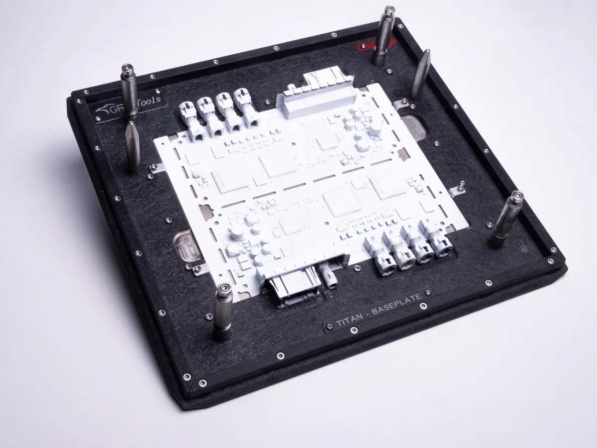
What a wave solder pallet does
The pallet carries the board through the machine and controls exactly where solder is applied. A good pallet protects sensitive areas, supports the board against warpage, and survives thousands of cycles without losing tolerance. The design — clearances, chamfers, hold-downs, material — is what separates a pallet that works from one that doesn't.
Where they're used
- Through-hole (THT) soldering on wave lines
- Selective masking on mixed-technology boards
- Protecting connectors, press-fit zones and keep-out areas
- Carrying thin or irregular boards that can't run unsupported
Materials — chosen for the job
Composite materials
Thermal stability and dimensional accuracy for the pallet body.
Titanium inserts
Where precision, wear resistance and long tool life matter most.
On request
Other materials matched to your temperatures, cycle count and budget.
Our process — from your data to series
- 01You send Gerber, STEP, DXF, ODB++ or HPGL, plus the target machine and panel/array layout.
- 02We design the pallet and confirm open points with you.
- 03We build and validate a prototype.
- 04We refine it with you, then move to serial production — with flexible revisions if your process changes.
What we need for a quote
Gerber, STEP, DXF, ODB++, HPGL, the target machine (e.g. wave or selective model), panel or single-board layout, expected quantities, and any keep-out or masking requirements. A physical PCB sample is helpful but not mandatory. NDA available on request.
RELATED PRODUCTS
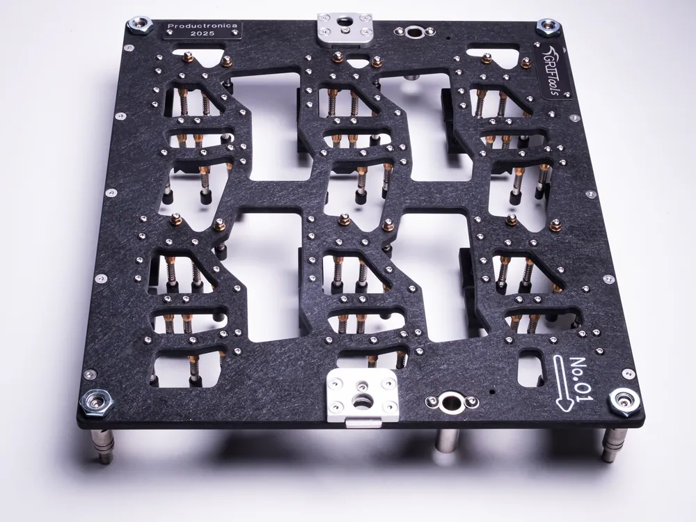
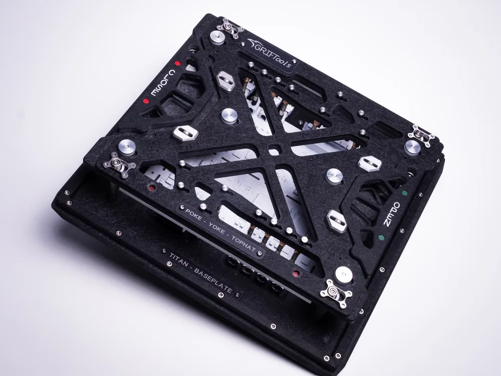
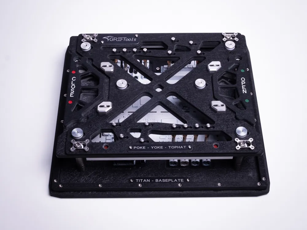
Common questions
What data do you need for a quote?
Gerber, STEP, DXF, ODB++ or HPGL, plus the target machine and panel layout. We'll tell you if anything else is needed.
Is a PCB sample required?
Usually not — Gerber/STEP/DXF/ODB++/HPGL is enough to start. A sample can help for complex boards.
What's the lead time?
Delivery time depends on complexity and quantity, and is confirmed with each quotation. As a general estimate, prototypes take 2–3 weeks, serial production around 5 weeks.
What material is the pallet made of?
Typically composite material, with titanium inserts where precision and wear matter.
Can you make small or first-article quantities?
Yes — we build and validate a prototype before any series run.
Can changes be made after the first trial?
Yes — flexible revisions after the prototype are part of how we work.
Do you ship internationally?
Yes — we serve customers across Europe and beyond.
Have a board and a process?
Send your data and we'll come back with a tailored quote — typically reviewed by a real engineer.